
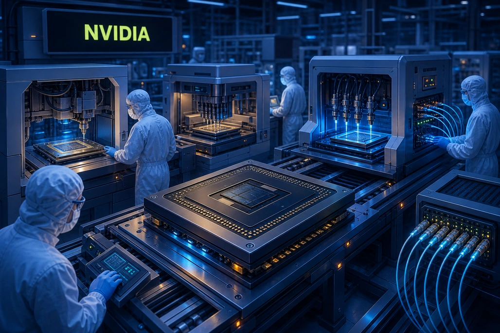
NVIDIA’s expansion targets multiple manufacturing stages needed to deliver AI infrastructure.
NVIDIA announced on October 21, 2026, that it is expanding manufacturing capacity with six supply-chain partners to support rising demand for AI infrastructure. For beginners, the important point is that an AI system is not produced by making a GPU alone: it also depends on specialized package substrates, advanced packaging, semiconductor testing and high-speed optical connections, each of which can limit how quickly complete AI servers can be delivered.
Key takeaways
- NVIDIA’s October 21, 2026 plan covers suppliers of substrates, advanced packaging, testing and optical engines rather than chip fabrication alone.
- The company targets a 2.5x increase in substrate capacity over the next three years through agreements involving IBIDEN, Samsung Electro-Mechanics and Unimicron.
- Amkor plans to expand interposer-wafer capacity by more than 300% by the end of 2028, according to NVIDIA.
- NVIDIA provided KYEC with a $1.1 billion capacity-reservation advance for new U.S. test facilities targeted for high-volume production in April 2027.
- SPIL is targeting a 15x increase in optical-engine capacity for co-packaged optics by mid-2027, followed by another planned doubling by the end of 2028.
What did NVIDIA announce?
At GTC Berlin on October 21, 2026, NVIDIA announced plans to expand global manufacturing capacity with Amkor Technology, IBIDEN, King Yuan Electronics (KYEC), Samsung Electro-Mechanics, Siliconware Precision Industries (SPIL), and Unimicron Technology Corporation. The program addresses four stages of the hardware supply chain: substrates, advanced packaging, testing and optical engines.
The central announcement is about capacity reservations and factory expansion. In a capacity reservation, a customer commits money or a future purchase relationship so a supplier can build equipment, production lines or facilities with more confidence that demand will exist when the capacity becomes available.
NVIDIA’s primary announcement frames the program as a response to production constraints in AI infrastructure. Independent coverage from The Elec and Tom’s Hardware similarly identified packaging, substrates, test and optical components—not just GPU fabrication—as the focus of the agreements.
This distinction matters because a finished accelerator system must move through many companies and manufacturing steps. A shortage at any one stage can delay a server even if the underlying GPU silicon is available.
Why are supply-chain components now important for AI infrastructure?
Modern AI systems combine compute processors, memory, networking hardware and power-intensive server components into dense systems. The result is that manufacturing the computing die is only one part of producing deployable AI infrastructure.
A useful beginner model is a relay race. A GPU designer may finish its part, but the system cannot reach customers until the package substrate is ready, the processor has been assembled in advanced packaging, the completed unit has passed testing, and the networking hardware can connect large numbers of systems. The slowest handoff determines the practical delivery pace.
NVIDIA has also disclosed in its August 2026 quarterly filing that it increased supply and capacity commitments from $119 billion to $279 billion as of July 26, 2026, to meet anticipated demand. The filing cautioned that land, power, buildings and capital are also necessary to deploy data-center infrastructure, so manufacturing expansion does not remove every constraint facing AI projects.
What is a package substrate?
A package substrate is a precision layer that connects a semiconductor package to the circuit board in a server. It provides the physical and electrical pathways that let a processor communicate with memory, networking and power-delivery components.
NVIDIA said its agreements with IBIDEN, Samsung Electro-Mechanics and Unimicron are expected to drive a 2.5x increase in substrate capacity over the next three years. IBIDEN’s Ono Plant in Japan is targeting three times its current capacity, with additional capacity expected to begin ramping in the first quarter of 2028.
Samsung Electro-Mechanics is joining NVIDIA’s substrate supply chain with existing South Korean capacity, facility upgrades and planned factories in Sejong and Busan. Unimicron’s KF substrate expansion in Taiwan is expected to begin adding capacity in the second quarter of 2027 and reach full capacity by mid-2028.
What is advanced packaging?
Advanced packaging is the process of assembling semiconductor components into a high-performance package. Rather than treating a processor as one isolated chip, advanced packaging can connect multiple components closely enough to operate as a tightly integrated system.
An interposer is one component used in some advanced packages. It acts as a dense connection layer between chips, helping link processors and other components inside the package. NVIDIA said Amkor plans to increase its interposer-wafer capacity in South Korea by more than 300% by the end of 2028.
Amkor announced a separate NVIDIA partnership in July 2026 that included a $1.5 billion multiyear advanced-packaging and development agreement supporting U.S. capacity expansion. Together, the announcements show why packaging has become a strategic part of the AI hardware supply chain rather than a final, interchangeable assembly step.
How do the six supply-chain partners fit together?
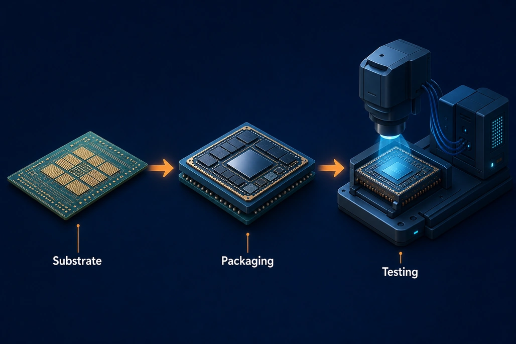
A complete AI system depends on every stage of the semiconductor supply chain.
| Partner | Supply-chain role in NVIDIA’s announcement | Planned capacity milestone |
|---|---|---|
| IBIDEN | Package substrates | Ono Plant targeting 3x current capacity; additional capacity expected to ramp in Q1 2028. |
| Samsung Electro-Mechanics | Package substrates | Existing South Korean capacity plus upgrades and planned Sejong and Busan factories. |
| Unimicron | Package substrates | Taiwan expansion expected to add capacity in Q2 2027 and reach full capacity by mid-2028. |
| Amkor Technology | Advanced packaging | More than 300% increase in interposer-wafer capacity targeted by the end of 2028. |
| KYEC | Semiconductor testing | New U.S. facilities supported by a $1.1 billion reservation advance; high-volume production targeted for April 2027. |
| SPIL | Optical engines for co-packaged optics | 15x capacity target by mid-2027, with another targeted doubling by the end of 2028. |
The table shows that the agreements address different constraints. Substrates connect a package to the wider system; packaging assembles complex semiconductor components; testing checks completed semiconductor products; and optical engines help deliver the high-speed connectivity needed as AI installations grow.
The geography is also diversified across Japan, South Korea, Taiwan, Singapore and the United States. NVIDIA described this as strengthening resiliency and redundancy, meaning it aims to reduce dependence on a single facility, region or production path.
How does semiconductor testing affect an AI server?
Semiconductor testing verifies that a completed product meets required electrical and functional standards before it becomes part of a server or networking system. Testing capacity therefore affects the number of finished, validated components that can move into final hardware production.
NVIDIA expects its total semiconductor testing capacity to double from calendar year 2026 to calendar year 2027 through buildouts in the United States, Taiwan and Singapore. The company said its $1.1 billion capacity-reservation advance to KYEC will support new U.S. testing facilities and equipment, with high-volume production targeted for April 2027.
NVIDIA also expects expanded testing operations in Singapore to begin high-volume production in February 2027. These are forward-looking targets, not completed production capacity; the company’s announcement explicitly notes that its plans and timing are subject to risks and uncertainties.
What are co-packaged optics and why is SPIL expanding them?
Co-packaged optics is a networking approach that brings optical components closer to the switching electronics that move data through a network. In this announcement, NVIDIA is focused on optical engines used in co-packaged optics for large-scale computing infrastructure.
AI factories and large AI clusters require many systems to exchange data. As clusters become larger, the network connecting processors, storage and switches becomes a major part of the overall system design. NVIDIA’s plan with SPIL is therefore about increasing the manufacturing capacity for an infrastructure component needed alongside compute hardware.
SPIL is targeting a 15x increase in optical-engine manufacturing capacity in Taiwan by mid-2027, with an additional doubling targeted by the end of 2028. The magnitude and timing are company targets rather than guarantees, but they show that NVIDIA is planning beyond processor supply alone.
When is the new capacity expected to become available?
The announced expansion is staged rather than immediate. Some capacity comes from existing operations, while factory construction, equipment installation and qualification will take place through 2027 and 2028.
| Date or period | Targeted milestone |
|---|---|
| February 2027 | Expanded Singapore testing operations expected to begin high-volume production. |
| Second quarter of 2027 | Unimicron’s Taiwan substrate expansion expected to begin adding capacity. |
| April 2027 | KYEC’s new U.S. testing facilities targeted for high-volume production. |
| Mid-2027 | SPIL optical-engine capacity targeted to reach 15x its starting level. |
| First quarter of 2028 | Additional IBIDEN Ono Plant capacity expected to begin ramping. |
| Mid-2028 | Unimicron’s expansion expected to reach full capacity. |
| End of 2028 | Amkor’s more-than-300% interposer-wafer expansion and SPIL’s additional optical-capacity doubling are targeted. |
These dates help explain why supply-chain announcements are significant even though they may not change near-term product availability immediately. Semiconductor manufacturing capacity requires long lead times because facilities, specialized equipment, production processes and quality checks all have to be ready before volume output begins.
What are the trade-offs and risks of capacity reservations?
Capacity reservations can benefit both sides. Suppliers gain more certainty when deciding whether to invest in expensive equipment and facilities, while NVIDIA gains a clearer path to obtaining critical components during a period of strong demand.
The trade-off is commitment. If demand changes, factory construction runs late, equipment is delayed, or a technology transition shifts requirements, planned capacity may not arrive on the expected schedule or may not match future needs perfectly. NVIDIA’s announcement classifies its projections about capacity, timing and benefits as forward-looking statements rather than guarantees.
There is also a broader infrastructure limit. Even if component supply increases, AI data centers still need land, electrical power, buildings, cooling systems, networking deployment and financing. Developers evaluating AI platforms should understand that more component capacity can improve hardware availability, but it cannot by itself complete a data-center project.
How should beginners interpret this announcement?
Beginners do not need to become semiconductor specialists to understand the practical message: AI infrastructure is a full supply chain. Software developers consume cloud services, APIs and AI models, but the services depend on physical systems that must be assembled, tested and connected at scale.
For teams planning AI workloads, the announcement is a reminder to separate application planning from infrastructure assumptions. A model, SDK or framework may be available today, while access to sufficient compute capacity can still depend on the hardware supply chain and on the customer’s cloud, power and deployment choices.
The most useful vocabulary to retain is simple: substrates connect packages, advanced packaging assembles high-performance semiconductor systems, testing validates completed components, and optical engines support high-speed networking. NVIDIA’s October 2026 program expands capacity across all four areas because each is necessary to deliver AI infrastructure at volume.
Frequently asked questions
What did NVIDIA announce on October 21, 2026?
NVIDIA announced capacity-expansion plans with Amkor, IBIDEN, KYEC, Samsung Electro-Mechanics, SPIL and Unimicron across substrates, advanced packaging, testing and optical engines for AI infrastructure.
Why is advanced packaging important for AI chips?
Advanced packaging assembles semiconductor components into a high-performance package, making it a necessary production stage for complex AI hardware. NVIDIA said Amkor is targeting more than a 300% increase in interposer-wafer capacity by the end of 2028.
What is NVIDIA’s $1.1 billion agreement with KYEC for?
NVIDIA said the $1.1 billion capacity-reservation advance will support KYEC’s new U.S. semiconductor-testing facilities and equipment, with high-volume production targeted for April 2027.
What are co-packaged optics?
Co-packaged optics is a networking approach that places optical components close to switching electronics. NVIDIA and SPIL are expanding optical-engine manufacturing capacity for this type of large-scale AI infrastructure connectivity.
Are NVIDIA’s capacity targets guaranteed?
No. The announced dates and capacity increases are forward-looking targets. NVIDIA states that actual results can differ because of manufacturing, market, technology, economic, regulatory and other risks.
Sources
- NVIDIA — NVIDIA and Supply Chain Partners Expand Capacity to Accelerate AI Infrastructure Buildout, October 21, 2026
- Amkor Technology — Strategic Partnership With NVIDIA to Expand Advanced Packaging and Test, July 23, 2026
- The Elec — Nvidia Invests in AI Supply Chain to Expand Production Capacity, October 22, 2026
- Tom’s Hardware — Nvidia Bankrolls AI Accelerator Supply-Chain Buildout to Reserve Production Capacity, October 27, 2026
- NVIDIA — Quarterly Report on Form 10-Q for the quarter ended July 26, 2026, August 27, 2026

Join the conversation! Your thoughts help the community grow.